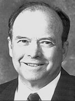


Dr. Robert W. Bower was born in Santa Monica, CA and is an applied physicist. Immediately after receiving his Ph.D. from The California Institute of Technology in 1973, he worked for over 25 years in many different professions: Engineer, Scientist, Department Head at University of California, Davis, and as president and CEO of Device Concept Inc. He also served as the President of Integrated Vertical Modules, which focused on three-dimensional, high-density structures. His most notable contribution, however, is his field-effect device with insulated gates—also known as a self-aligned-gate MOSFET (metal–oxide–semiconductor field-effect transistor), or SAGFET. Bower patented this design in 1969 while working at the Hughes Research Laboratories in Malibu, California. He has also published over 80 journals and articles, patented over 28 inventions, and authored chapters in 3 different books.
Early Life:
Robert W. Bower was born in Santa Monica, California in 1936. He remained in California throughout his life, except for 1954 – 1958 when he enlisted in the Air Force. After his service with the Air Force, he enrolled in UC Berkeley and in 1962 earned his A.B. in Physics while working at the Lawrence Radiation Laboratory. One year later, he earned his M.S. in Electrical Engineering from Caltech. In 1965, he worked in Malibu, California with Hughes Research Laboratories, which specializes in aerospace and defense operations. He later returned to Caltech and received his Ph.D. in Applied Physics in 1973. Currently, Dr. Bower is Professor Emeritus at the University of California, Davis, where he has been teaching for over 14 years.
At the Hughes Research Laboratories in the late 1960s, Bower strove to find the ideal element to integrate in all circuits. In 1920, Lilienfeld conceived of the basic design for this idea but had no platform to build or test his device. In the late 1950s, McCaldin and Hornoi devised of the silicon planar process and Kilby and Noyce established an Integrate circuit that could serve as a basic platform for Lilienfeld’s design. In 1963, Steven Hofstein and Frederic Heiman compiled the ideas from all previous scientists and were able to describe the fundamental nature of the MOSFET on a silicon planar process platform; however, they lacked one key asset that would power the MOSFET. In 1965, Bower conceived of the self-aligned-gate ion-implanted MOSFET which was the key to advances in integrated circuits.
The MOSFET (metal–oxide–semiconductor field-effect transistor) is a device that amplifies or switches electronic signals. However, without the self-aligned gate, the MOSFET lacked a proper source to improve the accuracy of the en\9.
Bower’s invention underwent much controversy when Kerwin, Klein, and Sarace argued that they were the actual inventors of the self-aligned gate transistors. In 1966, Bower and Dill presented the first publication the self-aligned gate transistor at the International Electron Device Meeting in Washington D.C.. That IEDM publication described the self-aligned gate transistor fabricated with both metal and polysilicon as the gate material and using both ion implantation and diffusion to form the source and drains. This was presentation 16.6 of this IEDM meeting. To Bower and to the attorneys who litigated the Bower U.S. 3,472,712 patent it was determined in the courts that his patent covered the general principal of using a gate as mask for both metal and polysilicon gates using ion implantation to establish the source and drain regions. Bower does not acknowledge the statement "Although Bower believed he was first in using aluminum as the gate and later developed the device using polysilicon as the gate, he was unable to prove it to the courts and the patent was awarded to Kerwin, Klein, and Sarace (U.S. 3,475,234)" is true. Actually is was the Hans G. Dill patent U.S. 3,544,3999, filed on October 26, 1966 that described the formation of the polysilicon gate self-aligned gate FET using diffusion of the source and drain that was disputed by the Kerwin et al. patent, not the Bower patent. It was also determined in a number of court cases that the vast majority of self-aligned gate FETs were made using ion implantation rather than diffusion to introduce the dopants into the source-drain regions. Bower conferred with the attorneys who litigated these cases and they confirmed that the statement "The US patent system grants the patent to the first developer of the invention, not the first one to be issued a patent." is not a valid statement of patent law.
National Inventors Hall of Fame, 1997
National Academy of Engineering, 1999