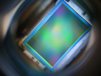


An active-pixel sensor (APS) is an image sensor consisting of an integrated circuit containing an array of pixel sensors, each pixel containing a photodetector and an active amplifier. There are many types of active pixel sensors including the CMOS APS used most commonly in cell phone cameras, web cameras, most digital pocket cameras since circa 2010, and in most DSLRs. Such an image sensor is produced by a CMOS (and is hence also known as a CMOS sensor), and has emerged as an alternative to charge-coupled device (CCD) image sensors.
CMOS active pixel sensor which includes a compensation circuit capable of compensating a lowered pixel voltage output due to leakage current of a photodiode. The CMOS active pixel sensor having a light sensing unit for generating an output voltage when light is incident thereupon, the sensing unit having an amount of leakage current before the incidence of light. A reset unit resets the output voltage of the light sensing unit to an initial reset voltage in response to a reset signal. A sense transistor has a source, a drain coupled to a power source voltage, and a gate coupled to the output of the light sensing unit. A select transistor has a drain connected to a source of the sense transistor, and provides the voltage of the sense transistor to a bit line, in response to a select signal. A compensation unit supplies a voltage corresponding to the output voltage of the light sensing unit lowered by the leakage current.
The term active pixel sensor was coined in 1985 by Tsutomu Nakamura who worked on the Charge Modulation Device active pixel sensor at Olympus, and more broadly defined by Eric Fossum in a 1993 paper.z
Invention History
Eric Fossum invented the image sensor that used intra-pixel charge transfer along with an in-pixel amplifier to achieve true correlated double sampling (CDS) and low temporal noise operation, and on-chip circuits for fixed-pattern noise reduction, and published the first extensive article predicting the emergence of APS imagers as the commercial successor of CCDs. Between 1993 and 1995, the Jet Propulsion Laboratory developed a number of prototype devices, which validated the key features of the technology. Though primitive, these devices demonstrated good image performance with high readout speed and low power consumption.
In 1995, personnel from JPL founded Photobit Corp., who continued to develop and commercialize APS technology for a number of applications, such as web cams, high speed and motion capture cameras, digital radiography, endoscopy (pill) cameras, DSLRs and camera-phones. Many other small image sensor companies also sprang to life shortly thereafter due to the accessibility of the CMOS process and all quickly adopted the active pixel sensor approach. Most recent, the CMOS sensor technology has spread to medium-format photography with Phase One being the first to launch a medium format digital back with a Sony-built CMOS sensor.